
Introduction
All soldering laboratories at TFix have high level of ESD-safe procedures and all circuit board as well as components are dealt in safest manner according to ANSI, IPC and JEDEC standards.
We suggest all our customers submitting boards to us or other component level repair laboratories take few simple steps to make sure the board isn’t exposed to potential damage to electrostatic shock during transit.
It is important to follow all HSE standards as well as JEDEC standards for Handling, Packing, Shipping and Use of Moisture/Reflow Sensitive Surface Mount Devices.
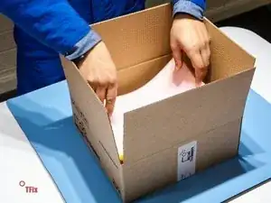
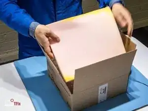
With high density printed circuit board assemblies consideration has to be taken to minimise the risk of flexing during transit. The board has to packaged in a rigid box with plenty of buffer material to ensure impact damage would cause minimal damage to the board.
-
-
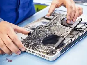
Safely remove components, such as digitiser and battery and disconnect all flex cables, which secure logic board inside the device. Correct tools and observation of all ESD precautions should be high priority due to sensitivity of the board.
-
-
-
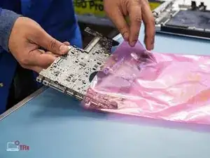
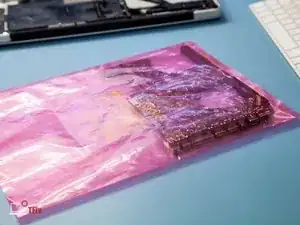
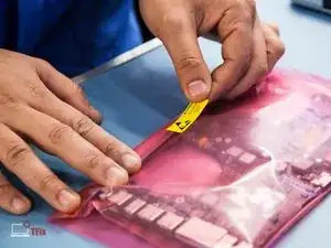
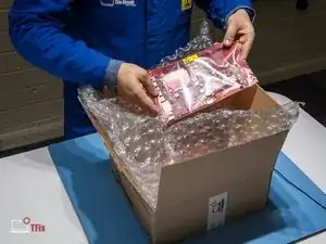
Please make sure ESD-safe packaging is used as All printed circuit boards requires to be within ESD-safe environment to ensure no damage will occur during handling whilst en-route. We suggest using pink bags, which can be acquired from all major electronic part retailers. ESD-precaution marking is a benefit.
-
-
-
Only rigid boxes with plenty of sufficient packaging to be used when transporting circuit boards to minimise the risk of shock or flex damage during transit. Make sure there is plenty of padding around the circuit board, however the board should not shift inside the box to prevent shock damage.
-


One comment
excelent very good
Rodrigo -