The 1 byte score is derived from two 4-bit instructions:
0000 0010
Explanation
The Motorola MC145008 is a single chip, one-bit, static CMOS processor optimized for decision-oriented tasks. The processor is housed in a 16-pin package and features 16 four-bit instructions. The instructions perform logical operations on data appearing on a one-bit bidirectional data line and data in a one-bit accumulating Result Register within the ICU. All operations are performed at the bit level.
The pins of the processor are numbered:
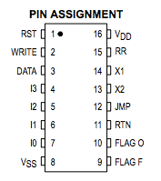
Instructions are presented to the chip on the 4 instruction pins, (I0, I1, I2, I3), and are latched into the Instruction Register, (IR), on the negative-going edge of X1.
In layman's terms, pins 4 through 7, are used to present the Instruction Register with an instruction, but the bits are interpreted in the reverse order. For example, the instruction 0001 would have pin #7 in the high state and pins 6 through 4 in the low state.
The instructions, are decoded in the Control Logic (CTL), sending the appropriate logic commands to the LU. Further decoding is also performed in the CTL to send a number of output flags (JMP, RTN, FLGO, FLGF) to pins 9 through 12. These are used as external control signals and remain active for a full clock period after the negative-going edge of X1.
Or, put simply, pins 9 through 12 are the output flags FLGF, FLGO, RTN, and JMP, respectively. Note that data is typically multiplexed to the WRITE pin (pin #2). The output flag pins are similar to other language's exit codes.
Each of the ICU's instructions execute in a single clock period.
Rotations
Initial position
0000    NOPO
0010    LDC
The clock periods:
- The
NOPO instruction puts pin #10 (FLGO) in the high state. Before the next clock period, the output flag pins are put back into the low state.
- The
LDC instruction loads the complement of the Data Bus' value to the Result Register, without affecting the output flag pins.
So, during the program's two clock periods, the output flag pins have represented 0100 0000, which, read in reverse (like the input pins), is 0000 0010, or the original instructions.
First rotation
0010    LDC
0000    NOPO
The clock periods:
- The complement of the Data Bus is loaded to the Result Register, with no effect of the output flag pins.
- Pin #10 in switched to the high state.
During these two clock periods, the output flag pins have represented 0000 0100, which, when reversed, are the instructions 0010 0000.


So I could have program
aaabbband I could say that the next rotation isbbbaaa? Or would the next rotation have to bebaaabb? – Beta Decay – 2017-05-19T09:30:42.8101The next rotation is
baaabb. – Leaky Nun – 2017-05-19T09:31:23.4601
Side note, the standard Fission quine is a different quine of rotation-safe: no matter how you rotate it, it will always print the original source code.
– Martin Ender – 2017-05-19T09:45:17.250I have a language that only recognizes eleven characters, and everything else is simply printed. Would this be considered cheating? – MD XF – 2017-05-29T04:36:45.547
1If a quine in a language is one byte, is that cheating? – MD XF – 2017-05-29T04:41:50.117
@MDXF If it's one byte it's not a proper quine in most cases. Well, some binary language might have a proper 1-byte quine, such as the first four bits identify the other four bits or something like that, but non-binary ones certainly don't. – Erik the Outgolfer – 2017-05-29T08:26:28.463
How 2D languages' code can be rotated? – Dead Possum – 2017-05-29T10:14:31.520
What about
ain PHP? Without<?phpit returnsa– Евгений Новиков – 2017-08-03T16:45:45.390Since you have no answers yet, you may consider allowing having either 'rotation softened' or 'rotation hardened' quines (i.e., output the original source or the rotated source). See my sandbox post which turned out to be a dupe of this challenge.
– Sanchises – 2017-08-09T20:10:56.837Just got one: ಠಠ in ಠ_ಠ, seems valid. (I do not want post it as answer, since i cannot understand what happening)
– tsh – 2017-09-05T05:37:54.3271
Is this a proper quine?
– tsh – 2017-09-05T05:50:45.767